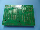
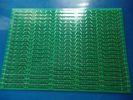
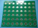
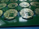
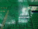
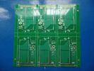
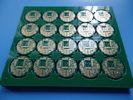
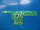
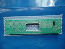
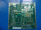
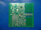
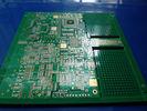
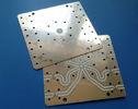
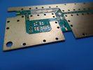
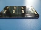
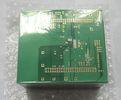
Black Double Sided Printed Circuit Boards 2 Layer PCB for Bluetooth Receiver - BIC-B1455-RE1
Black Double Sided Printed Circuit Boards 2 Layer PCB for Bluetooth Receiver For Sale, Most Competitive Price, Fast Delivery, Custom Service, Wholesale Black Double Sided Printed Circuit Boards 2 Layer PCB for Bluetooth Receiver, Made in China, High Quality Products!, China cheap prodocuts, china suppliers Supplier, Manufacturer.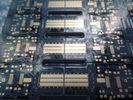
Black Double Sided Printed Circuit Boards 2 Layer PCB for Bluetooth Receiver
?
PCB Data sheets
- - - -
PCB SIZE | 250 x 236mm=50PCS |
BOARD TYPE | |
Number of Layers | Double sided PCB, 2 Layer PCB |
Surface Mount Components | YES |
Through Hole Components | YES |
LAYER STACKUP | copper ------- 35um(1oz)+plate TOP layer |
FR-4 1.5mm |
copper ------- 35um(1oz)+plate BOT Layer |
TECHNOLOGY | |
Minimum Trace and Space: | 8.5mil/6.5mil |
Minmum / Maximum Holes: | 0.3/0.9mm |
Number of Different Holes: | 2 |
Number of Drill Holes: | 1365 |
Number of Milled Slots: | 0 |
Number of Internal Cutouts: | 0 |
Impedance Control | no |
BOARD MATERIAL | |
Glass Epoxy: | FR-4, ITEQ IT-180 TG>170, er<5.4 |
Final foil external: | 1.5oz |
Final foil internal: | 0oz |
Final height of PCB: | 1.6mm ±0.16 |
PLATING AND COATING | |
Surface Finish | Immersion Gold (14.3%) 2micoinch over 100 microinch nickle |
Solder Mask Apply To: | Top and Bottom, 12micron Minimum |
Solder Mask Color: | Black, Kuangshun, SKM-S6189BK31 |
Solder Mask Type: | LPSM |
CONTOUR/CUTTING | Routing, Fiducial Marks, V-cut |
MARKING | |
Side of Component Legend | No silkscreen required. |
Colour of Component Legend | No silkscreen required. |
Manufacturer Name or Logo: | No silkscreen required. |
VIA | Plated Through Hole(PTH), via tented |
FLAMIBILITY RATING | UL 94-V0 Approval MIN. |
DIMENSION TOLERANCE | |
Outline dimension: | 0.0059& quot; |
Board plating: | 0.0029& quot; |
Drill tolerance: | 0.002& quot; |
TEST | 100% Electrical Test prior shipment |
APPLICATION: | Bluetooth receiver |
TYPE OF ARTWORK TO BE SUPPLIED | email file, Gerber RS-274-X, PCBDOC etc |
SERVICE AREA | Worldwide, Globally. |
- - - -
?
?
Advantages
a) High Tg FR-4. Industrial standard material with high Tg (175℃ by DSC) and excellent thermal reliability.
b) Immersion gold. SMT process is resistant to reflow soldering, resistant to rework.
c) Devlivery on time: >98%
d) Customer complaint rate: <1%
?
?
More Applications in Electronics
Gsm
Server
Hdmi Splitter
Outdoor Lighting
Routers
Low Noise Rf Amplifier
Custom Power Supply
Ac To Dc Power Supplies
Power Supply Socket
Security Access Systems
?
?
PCB knowledge: ENIG
ENIG stands for Electroless nickel immersion gold which is a type of surface plating used for circuit boards. It consists of an electroless nickel plating covered with a thin layer of immersion gold. Normally, the thickness of nickel is 120μ” - 200μ” (3μm to 5μm ) and gold 1-5μ” (0.025μm – 0.127μm).
?
ENIG has several advantages than HASL, including
a) Excellent surface planarity, particularly helpful for PCBs with BGA packages or even CSP mounted components to reduce failure rate during assembly and soldering.
b) Good oxidation resistance and good heat dissipation.
c) Long storage time ( It can be stored for more than 1 year in vacuum bag)
d) High solderability, no stressing of circuit boards and less contamination of PCB surface.
e) SMT process is resistant to reflow soldering, resistant to rework.
?
?
FAQ
How to Pay?
We accept bank wire transfer, Paypal. It& acute;s sorry, we currently do not accept credit card.
?
BICHENG ENTERPRISE LIMITED
Address: 3 203 Shidai Jingyuan Fuyong Town, Shenzhen, Guangdong, China, 518000
Tel: 86-755-27374946
Bicheng Enterprise Limited is an established supplier of printed circuit boards(PCBs) in Shenzhen, China. We specialise in printed circuit board with epoxy glass material (FR-4 grade), high frequency material and metal core substrate. Our PCBs have found ready markets in more than 100 countries and regions in the world.
We have very rich circuit board products. From a simple one to a complex PCB, a rigid one to a flexible PCB, prototype to production up to 32 layers, single material to hybrid construction, phenolic paper laminate to metal core base, normal multilayer to impedance control, through hole to blind via, ball grid array (BGA) to via in pad (VIP) and so on.
Our PCB produtcs are used for a variety of purposes, including, but not limited to, computer networking, safety and surveillance, power supply, Telecommunications, Industrial Automation, RF and Microwave, Automotive Electronics, Satellite Equipment and LED Lighting etc.

