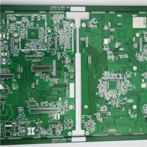
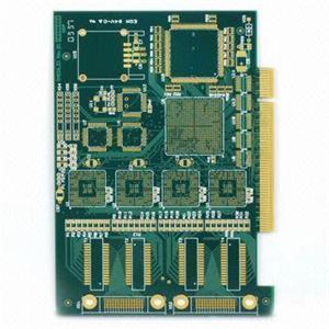
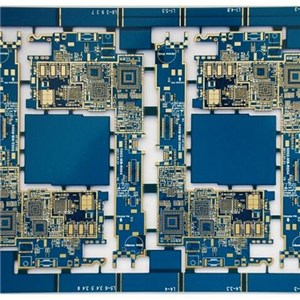
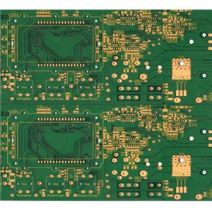
6 Layer Microvia Pcb Board With 3oz Inner Copper - No.1-1
6 Layer Microvia Pcb Board With 3oz Inner Copper For Sale, Most Competitive Price, Fast Delivery, Custom Service, Wholesale 6 Layer Microvia Pcb Board With 3oz Inner Copper, Made in China, High Quality Products!, China 6 Layer Microvia Pcb Board With 3oz Inner Copper,HDI Pcb, Supplier, Manufacturer.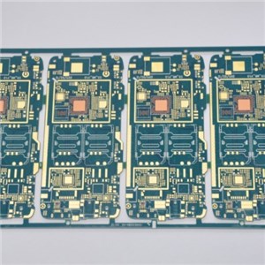
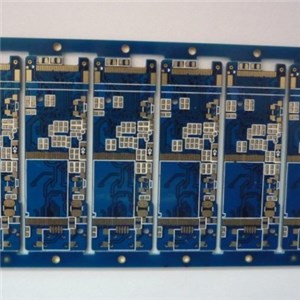
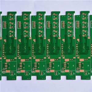
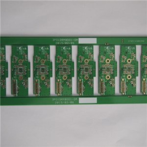
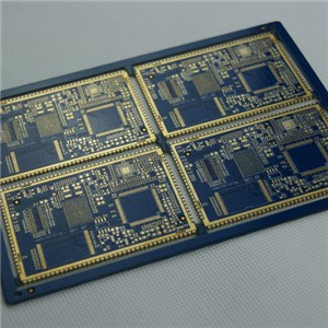
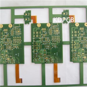
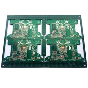
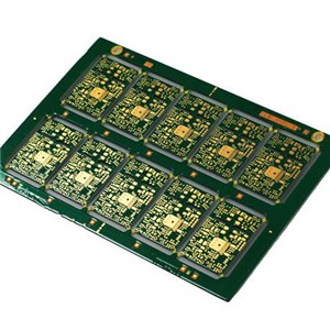
what& acute;s HDI pcb board ?HDI is High Density interconnect (High Density Interconnector) abbreviation, is one of the production of printed circuit board, using micro buried blind hole technology of a circuit board connect to more high density circuit line.PCB board SpecificationsPcb thickness:1.6mmLayer account:6LSurface finished:immersion gold+blind and bury via hole;Line width&space3/3milsFinished copper:1ozSolder mask:blue;Material:FR4.Certificates:CQC,ISO.TS16949,SGS,ISO9001,UL,ISO.14001,ROHSDelivery time:sample 3-5days,mass production:12-15days;Package details:vacuum pcb,inside bubble all inside,cartoon,ties outside strengthening;KDPCB Advantages1--never set any moq for every pcb board order;2--shortest response for all clients need;3--reasonable competitive price with high quality;4--support & quot;one-stop& quot;service for part of clients;5--shortest delivery time on pcb board production;6--& quot;5S& quot;and ISO.TS16949 quality system control manufacture;7--professional,high communication,trustworthy;8--all kinds of pcb board manufacture are acceptable;9--TNT/UPS/DHL/FEDEX/special shipping agency support with lower price;HDI pcb advantage1)can reduce the cost of PCB: after more than eight layer plate with HDI manufacturing, the cost will be lower than traditional pcb board manufacture;2)Increase the line density: interconnection of traditional circuit board and parts;3)For the use of advanced packaging technology;4)Have a better performance and accuracy of the signal;5)Reliability is better;6)Can improve thermal properties;7)Can improve the rf interference/electromagnetic interference/(RFI/EMI/ESD), electrostatic discharge;8)To increase design efficiency;9)Ability to?meet the density constraints of lines and pads on a typical design without increasing the layer count or board size;kdpcb?has years of experience in manufacturing HDI PCBs with Blind & Buried Vias. Both our engineers and production facility?are equipped to handle the intricacy this technique requires, with very high accu
Get QuoteMeizhou KeDing Industrial Co.,Ltd
Address: R203,xinbaosheng B,Xixiang bao鈥檃n district shenzhen city CHINA, shenzhen, guangdong, China, 518102
Tel: 86-755-29602597
MeiZhou KeDing Industrial Co.,Ltd is a rapid expansion PCB manufacturer that is aiming for multi variety PCB銆丩ow/Mid/High mix valume PCB production,Website:http://www.kd-pcb.com,which factory is located in AD5 area in dongsheng industrial park of economic development zone in meizhou city.
KDPCB has rich experiences in multilayer boards,thick copper boards,high temperature boards,high frequency boards and Aluminum boards etc.The production capacity is over 25000 square meters with various over 1000 items monthly.
Seventy percent of our products are exported to Europe,North America,and others countries which are widely applied in communication,industrial control,medical instrument,security electronics,consumer electronics and so on.
KDPCB insist the "customer-oriented, quality-centered" "pursue zero defect,perfect details"purpose.so far KDPCB obtained UL,ISO9001,ISO14001,ISO.TS16949,SGS,REACH certificates.KDPCB PCB products quality is consistent with European RoHs command,American IPC-A-600G Class 2 standard.
In order to serve our customers better future,KDPCB not only consider send our professional engineers to customer manufacturing base support,but also will consider establish our customer service centers in Germany and USA,South Africa.
http://www.kd-pcb.com

