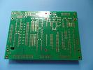
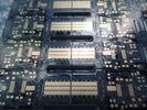
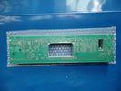
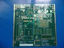
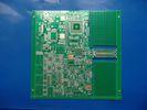
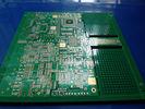
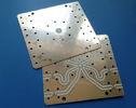
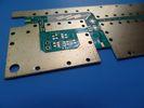
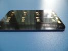
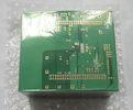
2 Layer High Tg PCB Immersion Gold Green Solder Mask For IR Module - BIC-1501-VER2.0
2 Layer High Tg PCB Immersion Gold Green Solder Mask For IR Module For Sale, Most Competitive Price, Fast Delivery, Custom Service, Wholesale 2 Layer High Tg PCB Immersion Gold Green Solder Mask For IR Module, Made in China, High Quality Products!, China cheap prodocuts, china suppliers Supplier, Manufacturer.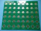
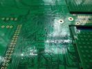
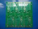
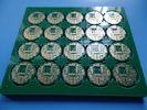
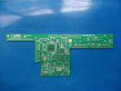
2 Layer High Tg PCB Immersion Gold Green Solder Mask For IR Module
?
PCB data sheets
- - - -
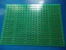
PCB SIZE | 190 x 190mm=48PCS |
BOARD TYPE | |
Number of Layers | Double sided PCB, 2 Layer PCB |
Surface Mount Components | YES |
Through Hole Components | no |
LAYER STACKUP | copper ------- 35um(1oz)+plate TOP layer |
FR-4 1.5mm |
copper ------- 35um(1oz)+plate BOT Layer |
TECHNOLOGY | |
Minimum Trace and Space: | 8mil/8mil |
Minmum / Maximum Holes: | 0.7/2.1mm |
Number of Different Holes: | 3 |
Number of Drill Holes: | 653 |
Number of Milled Slots: | 84 |
Number of Internal Cutouts: | 0 |
Impedance Control | no |
BOARD MATERIAL | |
Glass Epoxy: | FR-4, ITEQ IT-180 TG>170, er<5.4 |
Final foil external: | 1.5oz |
Final foil internal: | 0oz |
Final height of PCB: | 1.6mm ±0.16 |
PLATING AND COATING | |
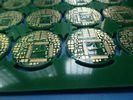
Surface Finish | Immersion Gold (15.3%) 2micoinch over 100 microinch nickle |
Solder Mask Apply To: | Top and Bottom, 12micron Minimum |
Solder Mask Color: | Gloss Green, Taiyo PSR-2000GT600D |
Solder Mask Type: | LPSM |
CONTOUR/CUTTING | Routing, Fiducial Marks |
MARKING | |
Side of Component Legend | TOP |
Colour of Component Legend | White, IJR-4000 MW300, Taiyo Supplied. |
Manufacturer Name or Logo: | Marked on the board in a conductor and leged FREE AREA |
VIA | Plated Through Hole(PTH), via tented |
FLAMIBILITY RATING | UL 94-V0 Approval MIN. |
DIMENSION TOLERANCE | |
Outline dimension: | 0.0059& quot; |
Board plating: | 0.0029& quot; |
Drill tolerance: | 0.002& quot; |
TEST | 100% Electrical Test prior shipment |
APPLICATION: | IR module |
TYPE OF ARTWORK TO BE SUPPLIED | email file, Gerber RS-274-X, PCBDOC etc |
SERVICE AREA | Worldwide, Globally. |
- - - -
?
?
Advantages
a) High Tg material. Excellent thermal reliability and CAF resistance providing long-term reliability for industrial and automobile application.
b) Lead-Free Assembly Compatible, RoHS compliant and suitable for high thermal reliability needs, and Lead free assemblies with a maximum reflow temperature of 260℃
c) Delivery on time. We keep higher than 95% on-time-delivery rate.
d) DDU Door to door shipment with competitive shipping cost. You don’t need to arrange anything after confirming the order. Just wait for your PCB delivery to your hand.
?
?
More Applications in Electronics
Wireless Speakers
TV Antenna
Gps Tracker
CCTV
USB Hub
Low Noise Amplifiers
Power Supply Replacement
Dc To Dc Transformer
Switching Dc Power Supply
Security Access Control Systems
?
?
MCPCB Capability
- - - -
NO. | Parameter | Value |
1 | Type of Metal Core | Aluminum, Copper, Iron |
2 | Model of Metal Core | A1100, A5052, A6061, A6063, C1100 |
3 | Surface Finish | HASL, Immersion Gold, Immersion Silver, OSP |
4 | Thickness of Surface plating | HASL: Sn>2.54μm, ENIG: Au 0.025-0.1μm, Ni 2.5-5μm |
5 | Layer Count | 1-4 Layers |
6 | Maximum of Board Size | 23& quot; x 46& quot; (584mm×1168mm) |
7 | Mininum of Board Size | 0.1969& quot; x 0.1969& quot; (5mm×5mm) |
8 | Board Thickness | 0.0157& quot; x 0.2362& quot; (0.4-6.0mm) |
9 | Copper Thickness | 0.5OZ(17.5μm),1OZ(35μm),2OZ(70μm),3OZ(105μm),4OZ(140μm) |
10 | Minimum Track Width | 5mil (0.127mm) |
11 | Minimum Space | 5mil (0.127mm) |
12 | Minimum Hole Size | 0.0197& quot; (0.5mm) |
13 | Maximum Hole Size | No limit |
14 | Minimum Holes Punched | PCB thickness <1.0mm: 0.0394& quot; (1.0mm) |
PCB thikness 1.2-3.0mm: 0.0591& quot; (1.5mm) |
15 | PTH Wall Thickness | >20μm |
16 | Tolerance of PTH | ±0.00295& quot; (0.075mm) |
17 | Tolerance of NPTH | ±0.00197& quot; (0.05mm) |
18 | Deviation of Hole Position | ±0.00394& quot; (0.10mm) |
19 | Outline Tolerance | Routing: ±0.00394& quot; (0.1mm) |
Punching: ±0.00591& quot; (0.15mm) |
20 | Angle of V-cut | 30°, 45°, 60° |
21 | V-cut Size | 0.1969& quot; x 47.24& quot; (5mm×1200mm) |
22 | Thickness of V-cut Board | 0.0236& quot; x 0.1181& quot; (0.6-3mm) |
23 | Tolerance of V-cut Angle | ±5o |
24 | V-CUT Verticality | ≤0.0059& quot; (0.15mm) |
25 | Minimum Square Slots Punched | PCB thickness < 1.0mm: 0.0315& quot; x 0.0315& quot; (0.8 x 0.8mm) |
PCB thickness 1.2-3.0mm: 0.0394& quot; x 0.0394& quot; (1.0 x 1.0mm) |
26 | Minimum BGA PAD | 0.01378& quot; (0.35mm) |
27 | Minimum Width of Solder Mask Bridge. | 8mil (0.2032mm) |
28 | Minimum Thickness of Solder Mask | >13μm (0.013mm) |
29 | Insulation Resistance | 1012ΩNormal |
30 | Peel-off Strength | 2.2N/mm |
31 | Solder float | 260℃ 3min |
32 | E-test Voltage | 50-250V |
33 | Thermal Conductivity | 0.8-8W/M.K |
34 | Warp or Twist | ≤0.5% |
35 | Flammability | FV-0 |
36 | Minimum Height of Component indicator | 0.0059& quot;(0.15mm) |
37 | Minimum Open Solder Mask on Pad | 0.000394& quot; (0.01mm) |
- - - -
?
?
FAQ
How do you control the quality?
We believe engineering design prevents problems from occurring in preproduction. Our PCB and Manufacturing process are certified by authorized organizations.
100% tests are inclusive of electrical test and AOI inspection, high voltage test, impedance control test, micro-section, solder-ability test, thermal stress test,
reliability test, insulation resistance test and ionic contamination test etc.
BICHENG ENTERPRISE LIMITED
Address: 3 203 Shidai Jingyuan Fuyong Town, Shenzhen, Guangdong, China, 518000
Tel: 86-755-27374946
Bicheng Enterprise Limited is an established supplier of printed circuit boards(PCBs) in Shenzhen, China. We specialise in printed circuit board with epoxy glass material (FR-4 grade), high frequency material and metal core substrate. Our PCBs have found ready markets in more than 100 countries and regions in the world.
We have very rich circuit board products. From a simple one to a complex PCB, a rigid one to a flexible PCB, prototype to production up to 32 layers, single material to hybrid construction, phenolic paper laminate to metal core base, normal multilayer to impedance control, through hole to blind via, ball grid array (BGA) to via in pad (VIP) and so on.
Our PCB produtcs are used for a variety of purposes, including, but not limited to, computer networking, safety and surveillance, power supply, Telecommunications, Industrial Automation, RF and Microwave, Automotive Electronics, Satellite Equipment and LED Lighting etc.

