Electronics Designing & Processing
Description
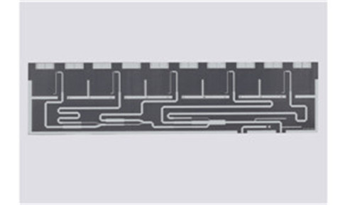
High Frequency PCB
1.
Product name: High frequency antenna board
cheap low volume pcb
Characteristic
1. using pure PTFE (PTFE) plate F4BM-2 production. the plate is relatively soft. in the production process is easy to deformation and size expansion and contraction;
2. need to use plasma processing;
3. the size of long. over most of the processing capacity of PCB factory;
4. non resistance welding design. line surface is easy to scratch. rub flower. the production process of the operation of the details have higher requirements.
5. due to the characteristics of the plate itself. the shape is easy to produce burr milling;
6. this kind of sheet is not recommended to do spray tin treatment. it is recommended to sink or sink tin treatment.
cheap pcb fabrication china
Specifications
Layer count: 2
Board thickness: 2.0mm
Base materials: F4BM-2
Finished size: 744*182mm
Surface finish:
tinLine width/line space: NA
Minimum hole: 0.40mm
Solder resist color: Non souder
Cu thickness: 1.5 OZ
Read More
China PCB Win Technology Co.,Ltd
Prototype PCBs, Quick Turn PCB, Middle-Low Volume PCBs, Special Technology PCBs, Aluminum PCBs, Custom Printed Circuit Boards
Address: JinYuan Building B-509,XiXiang Road No.300, XiXiang, Bao'an,ShenZhen,China,
ShenZhen, Guangdong
China, 518101
Tel: +86-755-23310576
Fax: +86-755-23310585
